1.3 VSWR of Cascaded Mismatches
1.3.1 INTRODUCTION
A broadband passive microwave component is normally characterised by its voltage standing-wave ratio (VSWR) and the insertion loss. These are measured at the design characteristic impedance Z0. The relationships between VSWR, component impedance, and return loss are:
VSWR = Zc/Z0, or Z0/Zc, such that VSWR>1
(1.3.1)
where Zc is the component impedance.
The reflection coefficient, ρ, is defined by
![]()
(1.3.2)
The component return loss (in addition to the component insertion loss) is equal to 20log(|ρ|), and the relationships between ρ and VSWR are
![]()
(1.3.3)
The convention for cascaded components has been to treat them as being effectively isolated. That is, only adjacent mismatches are considered with the insertion and VSWR losses being linearly accumulated. The overall VSWR is then estimated (Section 1.3.2) from the total return loss/reflection coefficient of the cascade thus formed.
This simplification does not take into account either the complex phasing of the returned vectors or, more importantly, the real mismatch of impedances between components. For instance, two transmission line components may have identical impedances and hence VSWRs. Cascading these components produces no reflection at the junction between them and therefore no change in the coupled VSWR. In most real situations the combined VSWR will also be a function of frequency and not be dependent upon only the component VSWRs but also on their complex impedances (Section 1.3.3).
Applet 1.3.1 Cascaded Mismatches
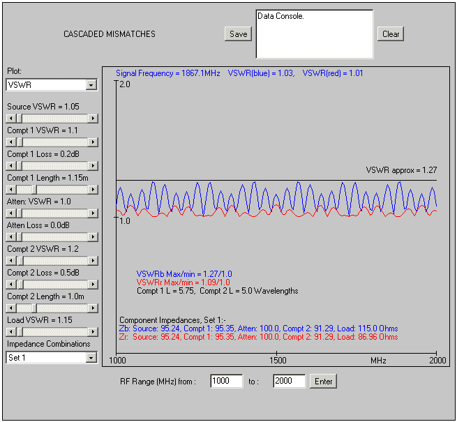
The applet applies the complex combination theory of Section 1.3.3 and calculates the VSWR or load power for a cascaded component chain. The chain comprises two variable electrical length transmission line components separated by a resistive attenuator, each are specified by VSWR and resistive insertion loss.
The example used in this applet comprises two components separated by an adjustable attenuator as shown in Figure 1.3.1. The components are specified by the VSWR, V, and insertion loss, L, from which, the reflection coefficient, ρ, and returned power, ρ2P, are derived.
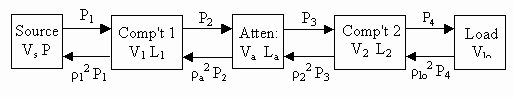
Figure 1.3.1 Linear Combination of Components
P1 is the available power from the source, and the power delivered to the load is

(1.3.4)
Using the linear combination method, the overall reflection coefficient is approximated by

(1.3.5)
from which the approximate overall VSWR can be calculated.
A better approximation is to obtain the source and load impedances at each junction to determine the VSWR and return losses before applying the above equations. Depending upon the impedance values, the junction mismatch can be either Va x Vb or Va/Vb.
1.3.3 COMPLEX COMBINATION
The correct approach to determine the cascaded circuit performance is to iteratively calculate the component input impedances in the complex domain from the component circuit parameters in the conventional way.
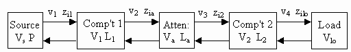
Figure 1.3.2 Complex Combination of Components
In Figure 1.3.2, zilo is the Load impedance; knowing this and Component 2 characteristics, the input impedance, zi2, to Component 2 can be calculated, as well as for the Attenuator, zia, and finally zi1, the loaded input impedance at Component 1.
The voltages in the cascade can then be found by working forward, starting from the source voltage Vs. In this example, Components 1 and 2 are assumed to be transmission line devices (a coaxial filter, for example) having a voltage transfer characteristic when loaded by an impedance zl of
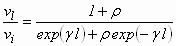
(1.3.6)
where:

zc is the component characteristic impedance.
γ =(α + jβ) is the component complex
attenuation and phase function.
l is the component electrical length.
The component input impedance is
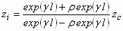
(1.3.7)
Note that for a transmission line device loaded by an impedance zl, evaluation of Equation 1.3.7 after substituting for ρ shows that the input impedance ranges from zi = zl, to zi = zc2/zl.
This means that, given the device worst-case input VSWR V, when terminated by the system design impedance z0, the implied transmission line characteristic impedance is either zc = z0√V, or zc = z0 /√V (applying Equation 1.3.1). When terminated by a resistance equal to the device characteristic impedance zc, however, the input VSWR improves to √V.
The T-attenuator transfer function is
![]()
(1.3.8)
where k is the attenuator attenuation factor, z0 is the design characteristic impedance, and zl is the attenuator load impedance.
The T-attenuator input impedance is

1.3.4 COMMENTS
The applet enables the accurate and the common approximate methods of calculating the effects of mismatch in broad band circuits to be compared. With five components, specified by just VSWR and insertion loss and measured at the system design characteristic impedance, there are 32 possible combinations of component impedances. These options can also be compared.
Interactively adjusting component VSWR and loss values illustrates how in worst cases even a few moderately mismatched components can give rise to large power variations in the load.
1.3.5 SELECTED BIBLIOGRAPHY
Engen, G.F., Microwave Circuit Theory and Foundations, London, England: Peter Peregrinus Ltd, 1992.
Pozar, D., Microwave Engineering, (2nd Ed.), New York: John Wiley & Sons, 1998.